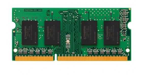
4GB 1600MHz DDR3 Non-ECC CL11 SODIMM 1Rx8
MYR103.00
IN STOCK
Brand: Kingston
Get shipping estimates
| Country | ||
| Region | ||
| Shipping Method | ||
|
|
||
MYR103.00
IN STOCK
Brand: Kingston
| Country | ||
| Region | ||
| Shipping Method | ||
|
|
||
 New
New
 New
New
MYR18.00
 New
New
MYR130.00
 New
New
 New
New
MYR299.00
 New
New
MYR129.00
 New
New
MYR85.00
 New
New
 New
New
 New
New
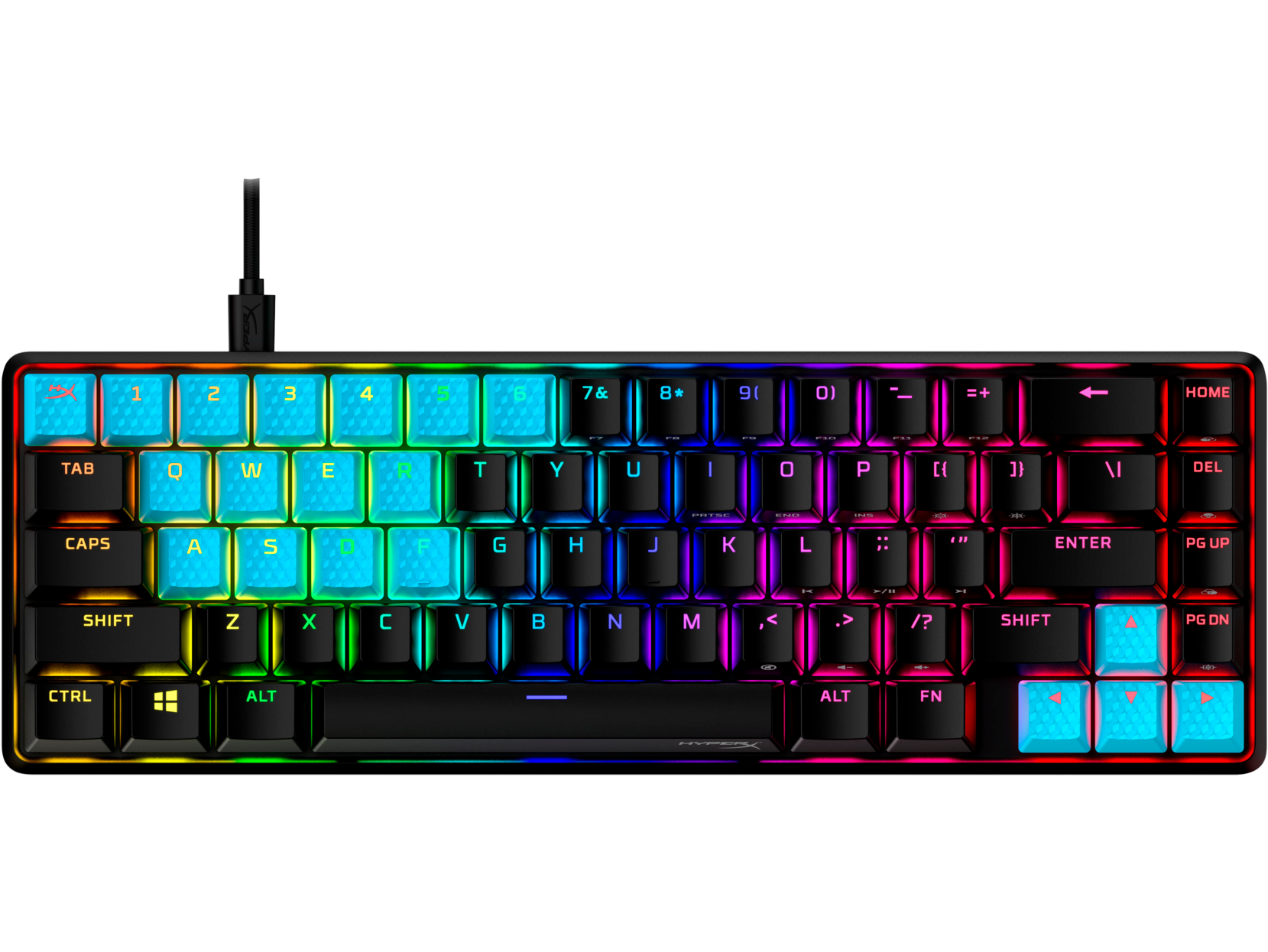
MYR362.95
 New
New
 New
New
 New
New
MYR102.00
 New
New
MYR359.00
 New
New
MYR410.00
 New
New
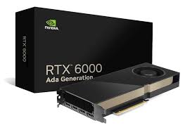
MYR632.00
 New
New
 New
New